About Us
One - stop Printed circuit board assembly Solution provider Keep Best PCB Assembly Co., Ltd serves many well-known brand customers in industrial control, security, medical, Internet of Things, automotive, artificial intelligence, smart home, power and communications industries at home and abroad. The company continues to be customer-centric, improves the level of digital intelligence, and is committed to meeting continued high-quality customer needs.
Get a free quote

Internet of Things
IoT PCBA Processing: Engineering Excellence for Connected Devices
As PCBA engineers at the forefront of IoT innovation, we understand that connected devices demand a unique blend of miniaturization, reliability, and technical precision. At [KEEP BEST], our expertise in IoT PCBA processing is rooted in solving the complex challenges of sensor integration, wireless connectivity, and low-power design—all while maintaining manufacturing scalability.

Advantages
-
& High-Density Manufacturing Leveraging 16 high-speed SMT lines, we excel in placing 01005 micro-components and 0.3mm pitch BGAs, achieving up to 16-up panel density for medical wearables and smart meters.
-
Low-Power & Thermal Management Optimization Our PMIC layout and thermal via designs reduce power consumption by 40% (e.g., smart agriculture sensor nodes) and support energy-harvesting interfaces for solar/piezoelectric power.
-
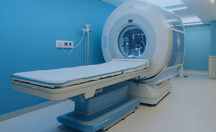
End-to-End Reliability QC System Implementing 19-step quality control including -40°C to +85°C temperature cycling, 85% RH humidity testing, and 100% X-RAY inspection, ensuring IoT gateways and outdoor devices withstand harsh environments.
The Engineering Challenges of IoT PCBA
Miniaturization & Density
IoT devices often require PCBAs smaller than a credit card, housing components like:
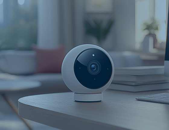
MEMS sensors for environmental monitoring (e.g., temperature, humidity, motion)
Sub-1GHz/2.4GHz wireless modules (Wi-Fi, Bluetooth LE, LoRaWAN)
Microcontroller units (MCUs) with embedded flash (e.g., ARM Cortex-M series)
Our 16 high-speed SMT lines excel in placing 01005 micro-components and 0.3mm pitch BGAs, achieving
panel densities up to 16-up in medical wearables and smart meters.

Power Efficiency & Thermal Management
Low-power designs are non-negotiable for battery-operated IoT devices. Our engineers optimize:
Power management ICs (PMICs) for ultra-low standby current (μA-level) Thermal vias and copper pours in PCB layers to dissipate heat from RF chips Energy-harvesting interfaces for solar or piezoelectric power sources
Case Study: For a smart agriculture sensor node, we reduced power consumption by 40% through optimized PMIC layout and low-leakage SMT component selection.
Power Efficiency & Thermal Management
Low-power designs are non-negotiable for battery-operated IoT devices. Our engineers optimize:
Power management ICs (PMICs) for ultra-low standby current (μA-level)
Thermal vias and copper pours in PCB layers to dissipate heat from RF chips
Energy-harvesting interfaces for solar or piezoelectric power sources
Case Study: For a smart agriculture sensor node, we reduced power consumption by 40% through optimized PMIC layout and low-leakage SMT component selection.
Connectivity & EMC Compliance
IoT PCBA must balance signal integrity with electromagnetic compatibility (EMC):
Impedance-controlled traces (50Ω for RF, 90Ω for differential pairs)
Shielded enclosures for wireless modules (e.g., nRF52840 Bluetooth chips)
Ground plane segmentation to isolate digital/analog domains Our in-line X-RAY and 3D SPI systems verify solder joint integrity in fine-pitch RF connectors, ensuring < 1dB insertion loss in 2.4GHz applications.
Engineering-Driven Solutions for IoT
Design for Manufacturability (DFM)
Our DFM process identifies IoT-specific risks:
Component coplanarity in 0201 passive components
Underfill voids in BGA packages for vibration resistance
Solder paste bridging in multi-row QFNs
Using Valor DFM software, we achieved a 99.7% first-pass yield for a smart home gateway with 1,200+ components.
Advanced Manufacturing Capabilities
16 SMT lines (Yamaha YSM20R) with 0.03mm placement accuracy
Nitrogen reflow for lead-free soldering of heat-sensitive sensors
Selective soldering for through-hole components in mixed-technology boards
Our Thailand facility specializes in high-volume IoT PCBA, offering 5-day turnaround for prototypes and 2-week lead times for mass production.
Quality Control for IoT Reliability
IoT devices operate in harsh environments, so we implement:
Temperature cycling (-40°C to +85°C) for industrial sensors
Humidity testing (85% RH) for outdoor monitoring equipment
Vibration screening (5-2000Hz) for automotive telematics units
Our 19-step QC process includes 100% X-RAY inspection of BGAs and automated functional testing (FCT) for wireless connectivity.
Partner with Our Engineering Team
For IoT innovators, choosing a PCBA partner means trusting in technical depth. Our engineers collaborate from concept to production, providing:
Free DFM/DFA analysis for IoT-specific designs
Component lifecycle management for long-term deployments
Post-production failure analysis with 3D X-RAY and AOI data
Contact us to discuss your next IoT project—from sensor nodes to edge computing gateways, we engineer PCBA solutions that define the future of connectivity.