About Us
One - stop Printed circuit board assembly Solution provider Keep Best PCB Assembly Co., Ltd serves many well-known brand customers in industrial control, security, medical, Internet of Things, automotive, artificial intelligence, smart home, power and communications industries at home and abroad. The company continues to be customer-centric, improves the level of digital intelligence, and is committed to meeting continued high-quality customer needs.
Get a free quote

PCB Stack - up Design Pitfall Avoidance Guide
-
KeepBestPcba
-
July 07, 2025
-
Comment()
PCB Stack - up Design Pitfall Avoidance Guide
What troubles you the most in each PCB design? Is it the dense traces or the mad
What troubles you the most in each PCB design? Is it the dense traces or the maddening EMI problems? The root of these issues may lie in a place you can't see - the PCB stack - up structure. When your design transitions from small - batch laboratory production to mass production, have you ever encountered a sudden deterioration in signal integrity? When the operating temperature of the product rises, does the PCB experience unexpected failures? These pain points most likely stem from an unreasonable stack - up design.
As we face increasingly high - speed circuit designs, a reasonable stack - up structure has become one of the key factors in the success or failure of a project.
Why is PCB stack - up design so crucial?
When choosing a stack - up structure, four key factors need to be balanced: product complexity, signal rate, EMC requirements, and cost budget. Here are the three core performances that it directly affects.
1. Signal Integrity
High - speed signal layers need to be sandwiched between power or ground planes to form a stripline structure. For example, when layer 3 is a high - speed signal layer, ground planes should be set above and below it.
2. Electromagnetic Compatibility (EMC)
A reasonable stack - up structure can reduce crosstalk by more than 60%. Multiple ground plane layers can effectively reduce the impedance of the PCB board and lower common - mode EMI.
3. Mechanical Stability
The stack - up must be kept symmetrical. Otherwise, differences in thermal expansion and contraction can turn the board into a "curved screen," and the soldering yield will drop significantly.
Selection of PCB Stack - up Schemes for Different Application Scenarios
1. Double - layer Boards: The Cost of a Low - cost Solution
Suitable for applications with simple structures and low signal rates, such as home appliance controllers and LED driver boards. It has obvious cost advantages, but poor EMC performance, and signals are easily interfered with. It is not suitable for complex wiring.
Design Tip: When space allows, try to increase the area of the ground wire to form a local reference plane.
2. Four - layer Boards: The Cost - effective Choice
For medium - complexity applications such as common MCU development boards and industrial control boards, four - layer boards are the best choice. The classic structure is TOP (signal) - GND - PWR - BOTTOM (signal).
The advantage is that the signal layers are close to the reference ground layer, which can effectively control impedance and reduce the length of the signal return path. It is suitable for digital circuit designs with differential signals or relatively high frequencies.
Advanced Technique: When the power layer is adjacent to the ground layer, control the inter - layer dielectric thickness between 0.1 - 0.2mm to reduce the impedance of the power plane.
3. Six - layer Boards: A Haven for High - speed Signals
When there are many high - speed signals (such as DDR4, PCIe), or the board has a small volume and high wiring density, six - layer boards are a better choice.
Recommended Structure: TOP - GND - Signal1 - PWR - GND - Signal2 - BOTTOM. This architecture sandwiches the high - speed signal layer (Signal1) between double - layer ground planes, achieving the best EMI suppression effect.
Cost Warning: Each additional layer may increase the cost by 50%, but the EMI risk can be reduced by 30%.
4. Eight - layer and Above: The Ultimate Solution for High - density Designs
Suitable for high - complexity BGA packages or ultra - high - speed systems. A typical solution is TOP - GND - Signal1 - PWR - GND - Signal2 - PWR - BOTTOM, with four signal layers and four reference planes.
Five Golden Rules for PCB Stack - up Design
1. Prioritize Signal and Power Integrity
High - speed Signal Layers: Prioritize placing them in the inner - layer stripline, with a distance from the reference plane ≤ 4mil.
Reference Plane Principle: Avoid signals crossing plane - divided areas, otherwise, the return path will be broken.
Differential Pair Handling: They must be routed on the same layer, with a length deviation ≤ 5mil, and avoid vertical wide - side coupling.
2. Symmetrical Design to Eliminate Stress
Copper Thickness Mirror Symmetry: For example, both L2/L3 layers use 1oz copper foil.
Symmetrical Distribution of Dielectrics: The dielectric thickness in the upper and lower halves is the same.
Special Treatment: For thick copper layers (≥ 2oz), the adjacent layers need a compensation design - for every 1oz increase in copper thickness, add 1 piece of PP on each side.
3. Material Selection Determines the Performance Ceiling
For harsh environments such as automotive electronics, choose materials with Tg ≥ 180℃, which can increase the reliability of the PCB by more than 30% under a temperature cycle of - 40℃ to 150℃.
4. Impedance Control is the Lifeline of High - speed Design
Accuracy Control: Use UV laser direct imaging (LDI) technology, with a line - width tolerance of ±0.2mil.
Manufacturing Compensation: For 1oz copper thickness, actually count it as 1.2mil in the model.
Special Boards: When Rogers and FR4 are co - laminated, use materials with the same coefficient of thermal expansion at symmetric positions.
5. Design for Manufacturability to Avoid Setbacks
PP Sheet Selection: Each dielectric layer should not exceed 3 PP sheets in the stack - up.
Thickness Control: The thickness of the PP dielectric between two layers ≤ 21mil (excessive thickness makes processing difficult).
Copper Foil Selection: For the outer layer, 0.5oz copper foil is preferred, and 1oz for the inner layer; select the power layer according to the current demand (2 - 3oz).
Practical Skills in the Manufacturing Process
1. Foil vs Core Lamination Method
Foil Method (copper foil laminated on the outer layer): Low cost, but difficult to control impedance (due to surface glue - flow problems).
Core Method (using core boards on the outer layer): 20% higher cost, but with high impedance accuracy.
2. Hybrid Material Lamination
When laminating Rogers and FR4, a stepped lamination process is required to prevent inter - layer slippage.
3. Thick Copper Board Manufacturing
For copper layers above 3oz, use the differential etching process - first etch to 2oz, and then perform secondary patterning to the target thickness.
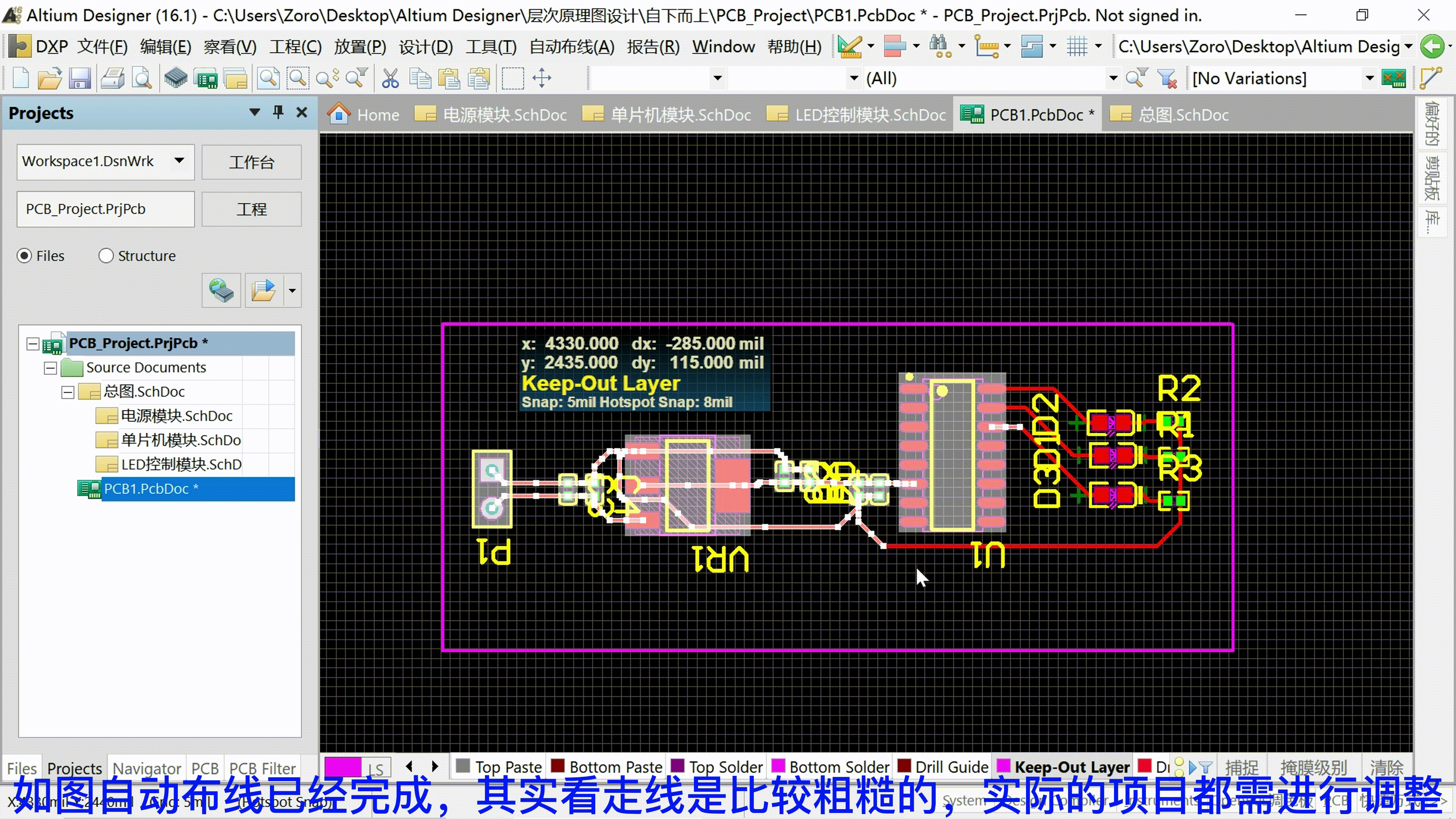
Key Step after Design Completion: Verify the Stack - up with Tools
After completing the stack - up design, how to verify it? The traditional method relies on the experience of engineers. Now, the KeepBestDFM software provides a one - stop solution.
1. Impedance Magic Tool
Combining various production factors, automatically calculate or inverse - calculate impedance to ensure that the impedance tolerance is controlled within ±10%.
2. One - click Analysis
Automatically detect design risks, eliminate production difficulties and design defects, and alert factors that affect the price.
3. Stack - up Verification
The software can automatically match a stack - up structure that meets production requirements, ensuring the reliable quality of multi - layer PCBs.
4. File Comparison
Easily compare the differences in stack - up between previous and current versions to avoid human oversight.
5. Design Tips
Pre - simulation can detect 80% of signal integrity problems. Combining the manufacturing analysis of KeepBestDFM can solve potential problems before production.
When you open the KeepBestDFM software and upload the design file, it's like giving your PCB stack - up a "full - body scan." The relevant manufacturing analysis indicators are跳动on the screen, and each item is related to the success or failure of the final product.
The software not only tells you where the problems are but also provides directions for optimization - whether it's adjusting the line width and spacing, modifying the stack - up structure, or even replacing with more cost - effective materials.
There is no one - size - fits - all answer for stack - up design, but with the assistance of professional tools, the new generation of hardware engineers no longer need to go through the painful cycle of "prototyping - failure - re - prototyping."
After completing the design, it's advisable to conduct a comprehensive check with KeepBestDFM to accurately locate potential problem areas and obtain reasonable optimization suggestions.
Recent Post

Leave a Reply
Your email address will not be published. Required fields are marked *